Wednesday 20 June 2012

Pharmaceutical Microbiology


1. a. Briefly describe the application of microbiology.
b. Briefly discuss about the contribution of i) AV Leeuwen-hoeck ii) Alexander Fleming
and iii) Louis Pasteur in Microbiology.
c. How can you test the sterility of a bacteriological media?
2, a. Define sterile products. Write down the name of some sterile products.
b. Define sterilization. Describe the process of autoclaving.
c. Describe the gram staining process of bacteria.
d. Write down the name of some gram-Positive and gram-negative bacteria.
3. a. What is peptidoglycan? Describe the composition and structure of the cell wall of
gram-positive and gram-negative bacteria.
b. Define Protoplast and Spheroplast.
c. What are flagella? Write down the composition and gram-negative bacteria.
4. a. Draw and label the structure of a lophotrichous bacteria.
b. What is bacterial chemotaxis? Describe the mechanism of bacterial movement.
c. Describe briefly the shape of bacteria.

Sunday 17 June 2012

Explain layered approach for the file system organization.


The file system itself is generally composed of many different levels.
The lowest level, the I/O control, consists of device drivers and interrupts handlers to transfer information between the memory and the disk system. The basic file system needs only to issue generic commands to the appropriate device driver to read and write physical blocks on the disk. Each physical block is identified by its numeric disk address. The file-organization module knows about files and their logical blocks, as well as physical blocks. This module also includes the free-space manager, which tracks unallocated blocks and provides these blocks to the file-organization module when requested.The logical file system uses the directory structure to provide the file organization module with the information the latter needs, given a symbolic file name. The logical file system is also responsible for protection and security.To create a new file, an application program calls the logical tile system. The logical file system knows the format of the directory structures. To create a new file, it reads the appropriate, directory into memory, updates it with the new entry, and  Layered File system. writes it back to the disk.

Three major methods of allocating disk space are in wide use. They are : contiguous, linked, and indexed. Each of them are explained below :


i) Contiguous allocation : The contiguous allocation method requires each file to occupy a set of contiguous blocks on the disk. Disk addresses define a linear ordering on the disk. The IBM VM/CMS operating system uses contiguous allocation because it provides such good performance.
Contiguous allocation of a file is defined by the disk address and length of the first block. If the file is n blocks long, and starts at location b, the it occupies blocks b. b+1, b+2, b+n-I. The
directory entry for each file indicates the address of the starting block and the length of the area allocated for this file.
One difficulty with contiguous allocation is finding space for a new file. A major problem is determining how much space is needed for a file.
To avoid several of these drawbacks, some operating systems use a modified contiguous allocation scheme, in which a contiguous chunk of space is allocated initially, and then, when that amount is not large enough, another chunk of contiguous space, an extent, is added to the initial allocation. The location of
a file's blocks is then recorded as a location and a block count, plus a link to the first block of the next extent.


Wednesday 13 June 2012

D.C. Bias and its Stabilization


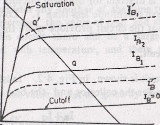
We have seen that for operation of a bipolar transistor as an amplifier, the emitter-base junction is forward biased and the collector-base junction is reverse biased. For amplification of an input signal and its faithful transfer to the load, (Lc. currents and voltages corresponding to a proper point in the linear region of the output characteristics are applied to the transistor. This point is defined 'cly particular values of In and VCE, or Ig and Ic, or Ic and VeE, and it is called the operating point, or quiescent point or Q-point.
When the operating point is established in the central region where the output characteristics are most linear and uniformly spaced, variations in input signal (base current) will produce proportional changes in output (collector current). In a good circuit design it is necessary that once the operating point is established, its position should not appreciably vary. If it shifts to a position near the saturation line or to a position near the cut-off region of the output characteristics, the signal, after amplification, by the transistor, will be distorted. In this chapter we consider various biasing methods for common-emitter amplifier circuits.
4.2. Factors which cause shift of the Operating Point.
The factors which cause shift in the position of the operating point are as follows :
(1) Parameter variations from unit to unit. There is usually a considerable spread in characteristics among transistors of the same type. The value of a may differ by a few percent from unit to unit of the same type. But this introduces a much wider spread into the factor (1—a) and hence into R. For example, suppose the value of a for a transistor is 0.98. The value of f3 for this transistor is


0.98
1 —0.98 —49.


If cc is 0.99 for a substitute transistor, then 13 for this transistor is 99. Thus a change in a by about 1% introduces a large change in p. There is also production spread in the collector leakage currents Icso and /cEo, and in the base-emitter voltage. Hence replacing a transistor in a given circuit may cause a large shift in the position of the operating point.
(2) Temperature variations.

D.C. Bias and its Stabilization


SCE E
Fig. 4-1.
Variation in temperature is a very important cause for shift in the position of the operating point. We have seen that the reverse leakage current IcB0 of the reverse-biased collector-base junction changes greatly with temperature, it approximately doubles for every 10°C rise in temperature. Therefore, an increase in temperature increases the value of Ics(). Since /c is related to /cso by the equation (See Sec. 3.7),
jc ----13/B+(13+1) !coo
an increase of /cao increases lc. Consequently all the output characterist'es are raised upward as shown by dotted curves in Fig. 4.1. Hence the operating point Q shifts upward towards the saturation line and the collector-current wave form will be distorted.
Another effect of rise of temperature of the transistor is called thermal runaway. An increase of temperature increases the leakage current IcgO. This increases the collector current Ic. The increase of Ic increases the power dissipated at the collector junction . and thereby increases the junction temperature.
Flicker noise


This is a: ether type of noise in transistor, and in other semiconductor deviczs. Its intensity is inversely proportional to the freqency. Therefore, it is also called semiconductor noise or 1/f noise. It has been observed that this noise becomes negligible above 1000 Hz. The cause for this noise is not completely understood. It is assumed that it originates in the irregular distribution and flow of carriers on the crystal surface in the vicinity of the depletion region. This noise increases with an increase of d c. voltage between the collector and the base. This noise in a transistor can be minimized by cleaning the crystal surface and by applying a smaller d c. voltage between the collector and base.
This noise is entirely absent in metals. Hence in electronic circuits where flicker noise is to be reduced wire-wound resistors are preferred to carbon resistors.

Basic Semiconductor Theory


In years before the Second World War solid state electronic devices were unknown. Vacuum tubes, magnetic amplifiers and relays were the only devices which were used in the processes of electrical signal generation, amplification, transmission, wave shaping and switching. After the invention of the transistor in - 1944 and subsequent development and improvement of the transistor and other solid state electronic devices, vacuum tubes are being replaced in many fields of applications, except in high-power
applications, by these solid state devices A solid state electronic
device consists of a semiconducting material and the development of a wide variety of semiconductor devices is due to wide range of electrical properties which a semiconductor acquires by minor chemical additions of some elements.
In this chapter we give a brief account of simple atomic theory of semiconductors.
11. Semiconductors.
The electrical resistivity of a good conductor like copper or
silver is very small, while that of an insulator is very large. F'or
example, the resistivity of silver is 1.6 x10⁻⁸ ohm-m and that of quartz is about 1012 ohm-rrt. - A semiconductor is a solid material whose electrical resistivity is higher than that of a conductor and lower than that of an insulator. Typical values of the resistivity of a semiconductor lie between 10-2 and 1 ohm m at room temperatures. This is not the only essential characteristic of a semiconductor. Other essential characteristics of a semiconductor are : -
(i) The electrical resistance of a semiconductor decreases with increase in temperature over a particular temperature-range which is charaCteristic of the semiconductor.

Per Amplifiers


The function of voltage amplifiers discussed in chapter 7 is to increase a signal voltage from a low level to a higher level which is required for operating some low-power circuit. Such amplifiers are generally operated under class A conditions so that the amplification is without distortion. The final stage of multi-stage amplifier is usually required to drive a loudspeaker or some load which requires sufficient power for its operation. Thus such a stage must supply large and undistorted power to the load. The final stage which does this function is called a large signal or a power amplifier.
A power amplifier is defined as a frequency converter which changes d.c. power into a.c. signal power. The input power is supplied by the d.c. source and the average power in the circuii is distributed according to the relation
d.c. power input=a.c power output-f losses.
A bipolar junction transistor that is suitable for a power amplifier is called a power transistor. It differs from other transistor in the following respects :
(i) The area of the collector region of a power transistor is large and the collector is attached firmly to a metallic heat sink so that heat, which is generated mainly in the depletion region between the collector and the base is taken away quickly.
(ii) In a power transistor the emitter and base layers are heavily doped and the contact area between the base layers and the base leads is in ring like form so that the area is increased. Consequently the ohmic resistance between the emitter and the base is very low. Because of this low resistance, a power transistor requires low input power, the saturation voltage in the output circuit becomes smaller and the current gain becomes more uniform.
Power amplifiers may be operated as class .4, class B, class AB, or class C. In this chapter we NN ill describe two classes of power amplifiers which are common in transistor circuits. They are class A, and class B push-pull power amplifiers.
In class A power amplifier the load is not directly connected in the collector circuit because of the following reasons. The quiescent current through the load resistance gives rise to a large wastage of power. If the load is the voice coil of a loudspeaker, a large d.c. quiescent current through the voice coil would cause damage to it. Hence in class A power amplifier the load is always coupled to the collector circuit by means of a transformer. Therefore, we will discuss class A power amplifier with transformer coupling only.
92. Transformer-Coupled class A Power Amplifier.
Dynamic speakers used in audio-amplifiers and in radio receivers are low impedance devices ; the voice coil of a loudspeaker is of the order of 10 ohms. The collector circuit of a power transistor has high impedance. Therefore, to transfer audio power from the collector circuit of the transistor to the speaker a voltage-step down and current-step up transformer is used.
The primary and secondary coils of the transformer are wound on an iron core and it is called an output transformer. The high impedance primary of the output transformer is connected in the high-impedance collector circuit and the low-impedance secondary is connected across the voice coil of the speaker. If RL is the impedance of the speaker, then according to the theory of an ideal transformer, the a.c. load impedance in the collector circuit will be
R' = 1, n2
Rr
number of turns of the.secondary N2
where number of turns of the primary N,
For a step-down transformer a is less than I.
The ratio is called the turns ratio of the
transformer. (The derivation of Eq. (I) is given at the end of this
section) Fig. 9.1 shows the circuit diagram of transformer coupled
class A power amplifier. The resistors R, and R2 provide potential
divider arrangement for forward biasing of the emitter-base

Tuesday 5 June 2012

Percentages of radio and television audiences


The given lines present the percentages of radio and television audiences over four years old in the UK from October to December 1992. Here, time of day or night is presented horizontally and percentages of population vertically. As is observed, radio and television audiences showed almost the opposite trend having showed a great variation in different times of day or night.
The bold graph here presents television audiences throughout the day. It shows that the percentage was zero in the early morning. But it gradually increased up to ten percent at 8.00 A. M. and remained almost the same with fluctuations up to 4. Then, the line went up very fast and attained its peak point, which was about fifty percent at around eight P. M. After that, the graph fell down pointedly and at four PM the percentage was below five percent, which was the lowest point. Then again a slow upward trend was observed.
On the other hand, the thinner graph describes the percentages of radio audiences. Unlike television, it started from just under ten percent and at eight A. M. attained the peak percentage amounting about 30%. After that, it gradually fell up to 4 P. M. intersecting the bold graph at around one P. M. However, a slight upward trend in the percentages was observed from four to six P. M.
As is observed, Television was much more popular than radio having the highest number of audiences summing almost 50 percent. The percentage is almost twice as much as Radio has. However, both the radio and Television had equal number of audiences at around 12 A. M. at which the two lines intersect each other.
In conclusion, it is clear from the lines that radio was very popular among the audiences in the early morning, on the other hand television got its highest percentage of onlookers in the evening.